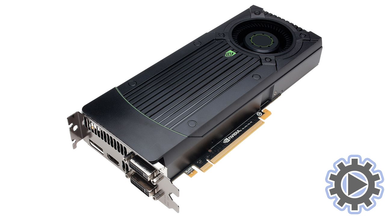
GeForce GTX 670
| Manufacturer: | NVIDIA |
| Series: | GeForce 600 |
| Codename: | GK104-325-A2 |
| Release date: | 2012. May 09. |
| Die count: | 1 |
| Die size: | 294 mm2 |
| Fab: | 28 nm |
| Transistors: | 3540 millions |
| Bus interface: | PCI-E 3.0 x16 |
Clock rates
| Core clock: | 915 MHz |
| Core clock (Boost): | 980 MHz |
| Shader clock: | 915 MHz |
| Memory clock: | 1502 MHz |
| Effective memory clock (DDR): | https://gamesystemrequirements.com/ 12016 MHz |
Memory
| Memory size: | 4096, 2048 MB |
| Memory bus type: | GDDR5 |
| Memory bus width: | 256 bit |
| Memory bandwidth (maximum): | 192.256 GB/s |
Core units
| Unified shader units: | 1344 |
| Texture mapping units (TMU): | https://gamesystemrequirements.com/ 112 |
| Render output units (ROP): | 32 |
| SM count: | 7 |
Supported Technologies:
| DirectX: | 12 |
| OpenGL: | 4.5 |
| OpenCL: | 1.1 |
| NVIDIA PhysX, NVIDIA Surround, NVIDIA TXAA, NVIDIA Adaptive Vertical Sync, NVIDIA 3D Vision Ready, NVIDIA SLI, NVIDIA G-SYNC |
Performance
| Pixel fillrate: | 29.3 (GP/s) |
| Texture fillrate: | https://gamesystemrequirements.com/ 102.5 (GT/s) |
| Thermal Design Power (TDP,Max): | 170 W |
| Release price (USD): | 400 USD |
Comments
Please login to post a comment.
Login
No comments have been posted. Be the first to comment!